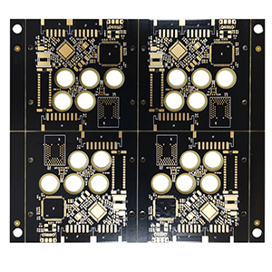

The HDI Rigid PCB is a high-density circuit board with micro-blind buried via technology. There are inner and outer circuits in the HDI board, and then drilling, metallization in the hole and other processes are used to complete the penetration and connection of the inner circuits of each layer.
Since HDI Rigid PCB is manufactured using a build-up method, it has the ability to make the end product design more compact. At present, it is widely used in mobile phones, digital cameras, notebook computers and so on.
We inspect the solderability and microsection of the HDI Rigid PCB according to the methods specified in standards such as IPC-S-804 to check the internal defects of HDI circuit boards.