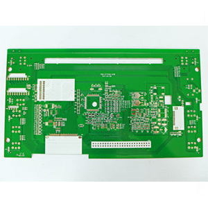

Of all multilayer types, the most common is the 4 layers rigid printed circuit board (PCB). The stack of 4 layers PCB is very rigid, including top layer, inner layer 1, inner layer 2 and bottom layer, which is used to route electrical signals. Two inner layers (inner layers 1 and 2) are located between the top and bottom layers. Therefore, the 4 layers rigid PCB means two signal layers + one positive voltage layer (VCC layer) + one ground layer (GND layer) or three signal layers + GND layer. In the 4 layers rigid PCB design, more surface area can be used for routing. Therefore, this design structure can provide excellent routing for low-speed and high-speed signals.
4). Lightweight structure.
9). Space probe equipment, etc.
We can tell from the appearance that the 4 layers rigid PCB needs to go through a variety of strict production and processing in the production process to meet the requirements. The printing ink on the appearance is covered in time, and there is no air oxidation condition on the copper surface. In addition, all the surfaces are invisible to meet the quality requirements.