
Lamination is the process of bonding layers of wires into a whole with the help of B-stage semi-cured sheets. This bonding is achieved through the interdiffusion, infiltration and interweaving of macromolecules at the interface. The process by which the layers of the circuit are bonded together as a whole. This bonding is achieved through the interdiffusion, infiltration and interweaving of macromolecules at the interface.
The biggest advantage is that the distance between the power supply and the ground is very small, which can greatly reduce the impedance of the power supply and improve the stability of the power supply. The disadvantage is that the impedance of the two signal layers is high, and because the distance between the signal layer and the reference plane is large, the area of signal backflow is increased, and EMI is strong.
Applicable to SMT BGA, CSP, Flip-Chip, IC semiconductor components, connectors, wires, photovoltaic modules, batteries, ceramics, and other electronic products internal penetration testing.
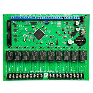
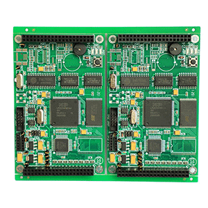
Multilayer DIP PCBA Multilayer DIP PCBA